
Now Reading: Scientists discover new way to grow materials on-demand using crystals and light
-
01
Scientists discover new way to grow materials on-demand using crystals and light
Crystals used in applications as varied as lasers, LEDs and the semiconductors used in sensors found in astronomical instruments could someday be ‘drawn’ rather than ‘grown’, leading to higher performance and lower costs.
A team led by Elad Harel of Michigan State University has used a laser to heat a gold nanoparticle, which then triggers crystal formation within a solution of lead halide perovskite. By moving the gold nanoparticle, again using lasers, it is therefore possible, in theory, to precisely ‘draw’ the crystals exactly where they need to be in an electronic device.
“In a device, one may need a very small quantity of crystalline material placed at very specific locations,” Harel told Space.com.
Harel’s new technique, using a phenomenon known as ‘plasmonic heating’, is able to regain some control over the formation of crystals. In laboratory experiments, Harel’s team fired a laser of 660 nanometers wavelength at a gold nanoparticle in a reaction chamber filled with the lead halide perovskite precursor solution over a glass substrate of borosilicate, onto which the crystal would be ‘drawn’.
The gold nanoparticle is tiny, less than one-thousandth of the width of a human hair. Therefore the entire procedure has to be extremely precise, and can be watched in real time using high-speed microscopes with frame rates of sub-millisecond timescales.
“The reason we use gold nanoparticles is because they act as small heaters,” said Harel. “When a laser irradiates the particle at the right frequency, it causes the electrons in the gold to oscillate, which generates heat.”
This is plasmonic heating and it drives the crystallization of the precursor solution in the exact locations that Harel’s team want it to.
Lead halide perovskite crystals exhibit high-performance in solar cells and LEDs, but they are not the only type of crystal used in electronics. For example, the semiconductors in the Mid-Infrared Instrument (MIRI) on the James Webb Space Telescope incorporate arsenic-doped silicon crystals. Harel hopes that this plasmonic heating technique can be applied to other such crystals, but it works for lead halide perovskites specifically because they have some rather unusual properties.
“What’s special about these perovskites is that as the temperature increases the solubility decreases, which induces crystallization,” he said. “Most materials do not exhibit this retrograde solubility property; typically as the temperature increases, the solubility increases.”

However, there may be a way around this that lies in the jiggling, excited electrons. As well as producing heat, the electrons could in principle also take part directly in the chemistry of crystal formation, according to Harel, encouraging crystal formation.
“We do need to do more work to generalize this concept to other materials, but we believe it will work,” he said.
The advantages of cheaper, faster and more precise crystal formation are clear to see. Crystals are used everywhere, from touchscreens, smoke alarms, solar panels, medical imaging devices, and most optoelectronics and photodetectors in general.
“This is a very simple method using low-cost lasers,” said Harel. “It also saves enormously on the cost of fabrication since the crystal could be placed exactly where and when it is needed.”
Given crystals’ importance to astronomical sensing, the technique of drawing them could even see lower-cost instruments launching on space missions in the future.
The next step is to use multiple lasers across a variety of wavelengths to try and ‘draw’ more intricate patterns of crystals, and then begin testing them in real devices to see if they really do offer a better standard of performance for less cost. “This is something we’re working on right now,” said Harel.
This new technique of ‘drawing’ crystals is published in the journal ACS Nano.


Related Posts

Stay Informed With the Latest & Most Important News
Previous Post
Next Post
Advertisement
-
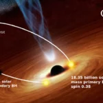 01Two Black Holes Observed Circling Each Other for the First Time
 -
 02From Polymerization-Enabled Folding and Assembly to Chemical Evolution: Key Processes for Emergence of Functional Polymers in the Origin of Life
 -
 03Astronomy 101: From the Sun and Moon to Wormholes and Warp Drive, Key Theories, Discoveries, and Facts about the Universe (The Adams 101 Series)
 -
 04True Anomaly hires former York Space executive as chief operating officer
 -
 05Φsat-2 begins science phase for AI Earth images
 -
 06Hurricane forecasters are losing 3 key satellites ahead of peak storm season − a meteorologist explains why it matters
 -
 07Binary star systems are complex astronomical objects − a new AI approach could pin down their properties quickly