
Now Reading: Technology Originally Developed for Space Missions Now Integral to Everyday Life
-
01
Technology Originally Developed for Space Missions Now Integral to Everyday Life


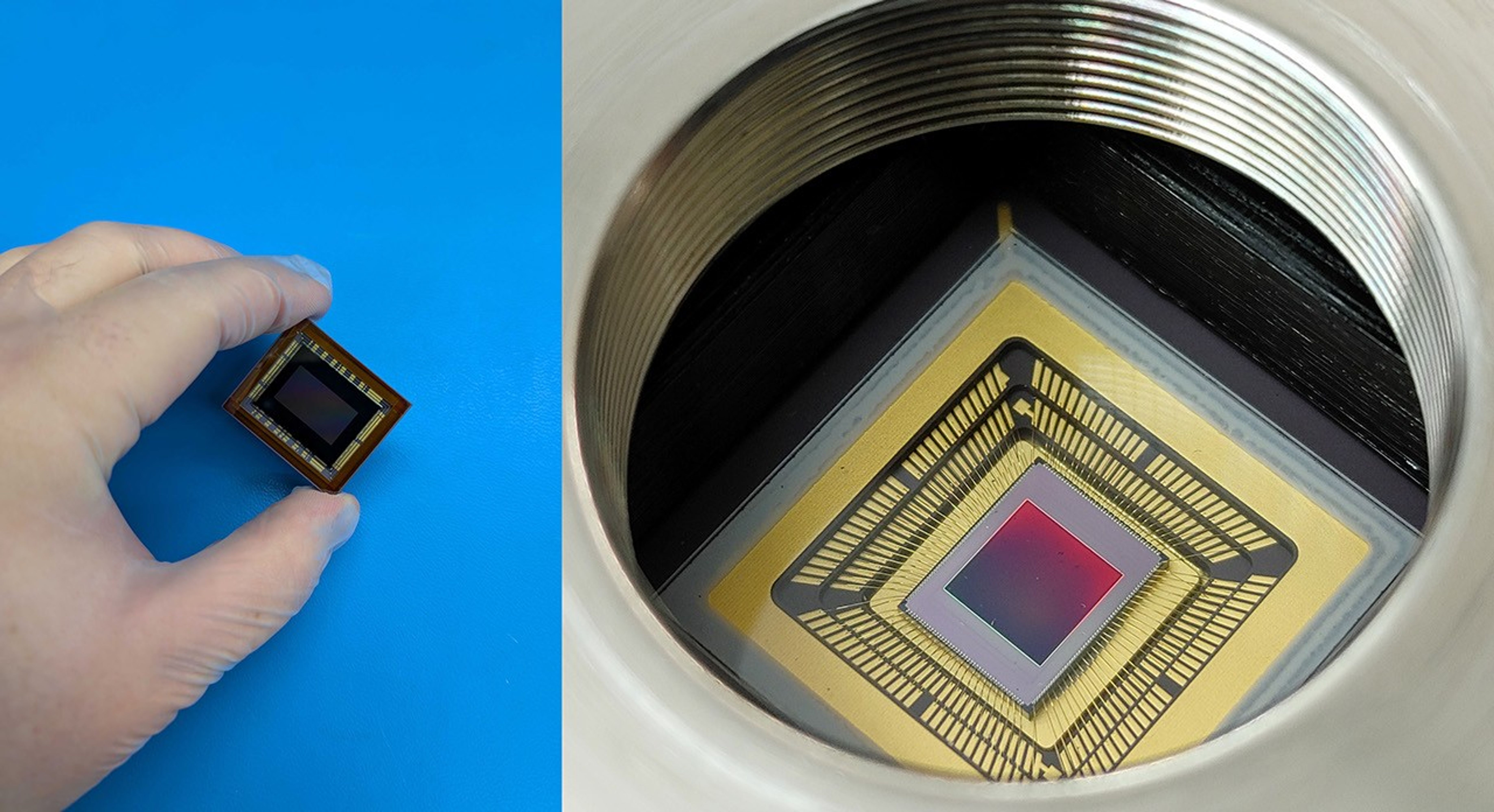
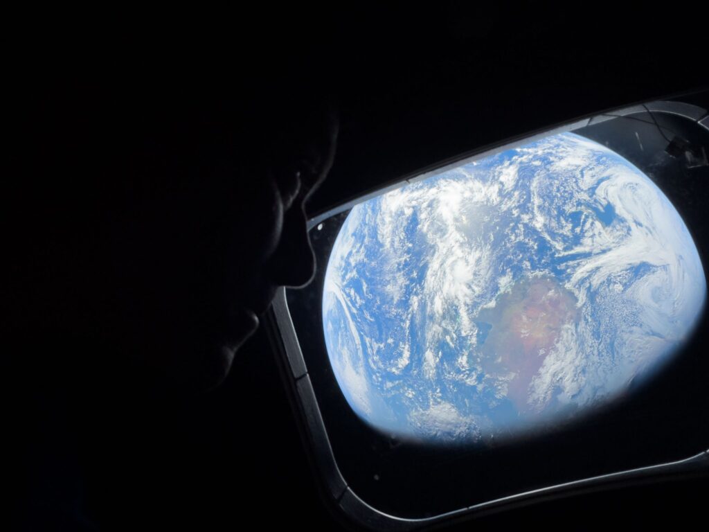
Groundbreaking “camera-on-a-chip” technology that was originally developed at NASA’s Jet Propulsion Laboratory (JPL) for use in space missions is currently employed in billions of devices like cell phones that are used daily by people worldwide.
In the 1980s, sensors used to produce high-quality images for space science (including the amazing images from NASA’s Hubble Space Telescope) and other applications employed charge coupled device (CCD) technology. Dr. Eric Fossum was originally hired at JPL in 1990 to advance CCD technology for use in interplanetary space missions, but he ended up advancing another technology called complementary metal-oxide semiconductor (CMOS) technology for that purpose and much more. While at JPL, Fossum took advantage of a technique commonly used for CCDs and applied it to CMOS sensors to develop the first CMOS active pixel image sensor. This development began a chain of events that led to the present use of CMOS technology not only in space science missions, but also in billions of cameras in smartphones, webcams, automobiles, and medical devices used worldwide.
A new technology emerges…
In 1990, CCDs were the primary technology used to generate high-quality images. CCD sensors consist of arrays of pixels that convert light into electric charges. The charge from each pixel is transferred step-by-step to an output amplifier at the corner of the sensor and converted to a voltage that represents the brightness of the light received at the corresponding pixel. The data from all the pixels is then aggregated to generate an image. While CCD cameras can produce very high-quality images that are suitable for scientific use, they require a lot of power and an efficient charge transfer process to be effective.
CMOS sensors, on the other hand, have signal amplifiers within each pixel and signals can be read directly from each pixel instead of being transferred long distances to an amplifier for conversion. CMOS sensors therefore require less voltage to operate than CCDs and issues with the charge transfer process such as radiation susceptibility are greatly reduced. Although CMOS sensors existed in the 1990s, they produced too much noise to produce high-quality images required for science applications.
To reduce the signal noise typical of CMOS sensors at that time, Fossum applied a technique that was often used in CCD devices. This technique—called “intra-pixel charge transfer with correlated double sampling”—enables a double measurement of a pixel’s voltage without and with the light-generated charge. Subtracting the values of these two samples enables noise to be suppressed, improving the signal-to-noise ratio.
The next steps
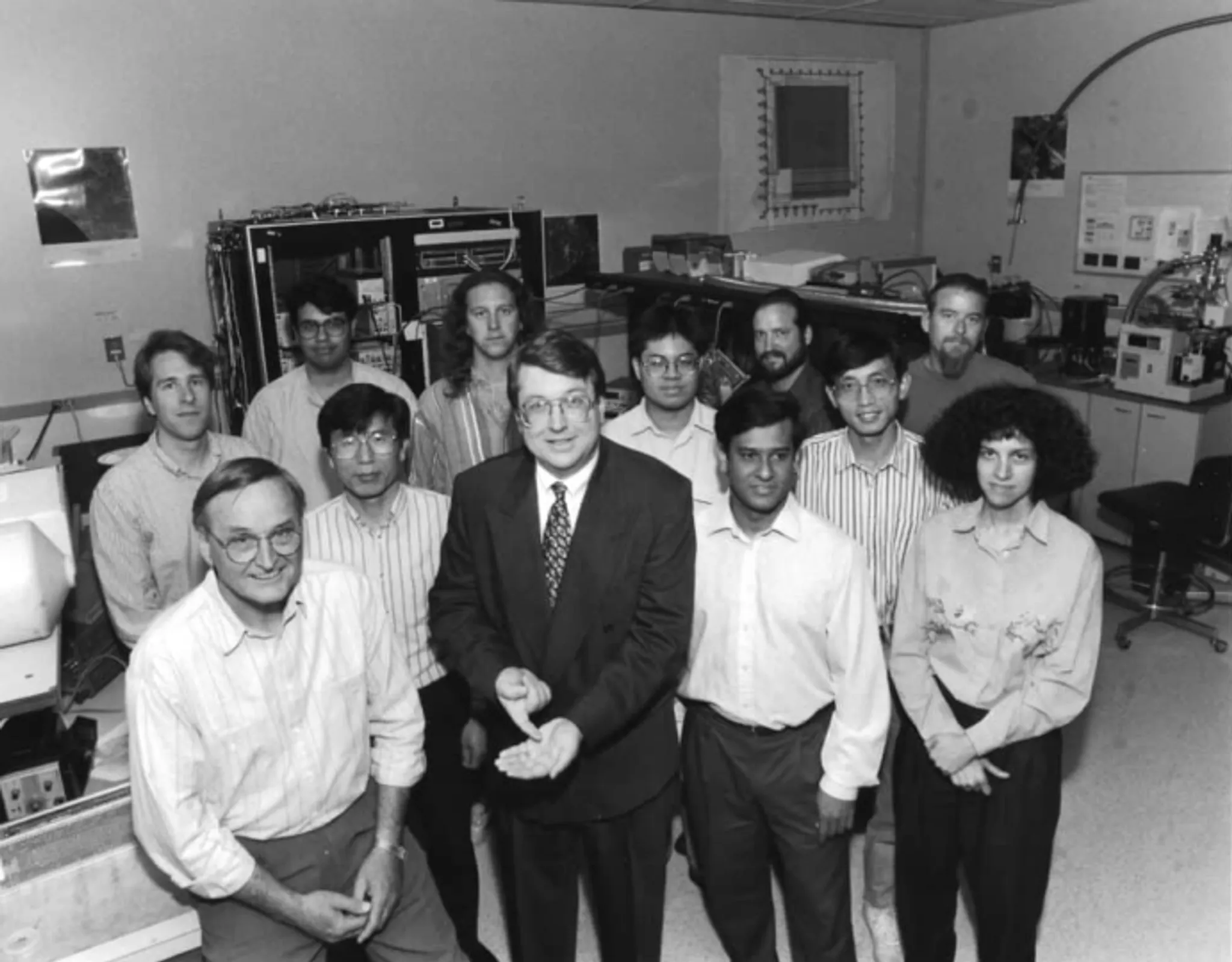
Soon several companies signed Technology Cooperation Agreements with JPL and partnered with Fossum and his colleagues to develop the promising new technology. In 1995, Fossum and co-worker Dr. Sabrina Kemeny licensed the technology from CalTech and founded a company called Photobit to develop CMOS sensors. In 1996, Fossum left JPL to work at Photobit full time. The Photobit, team further refined the CMOS technology to get it closer to CCD capabilities, reduce power requirements, and make manufacturing cheaper.
Shortly thereafter, CMOS cameras started to be used in webcams, “pill cams” (small, swallowable devices that incorporate a tiny camera to take thousands of high-resolution images of the digestive tract), and other applications. In 2001 Photobit was acquired by Micron Technology, a larger company that devoted even more resources to development of CMOS technology. With the subsequent explosion of the cell phone industry, by 2013 more than a billion CMOS sensors were manufactured each year, and today that number has grown to about seven billion per year.
Where are these sensors now?
The CMOS technology Dr. Fossum originally developed has not only enabled space science, it has been infused into devices we depend on every day, dramatically and positively transforming many aspects of our lives. Virtually all digital still and video cameras, including those on cell phones, employ them. In addition, CMOS technology is used in automotive electronics, webcams, sports cameras, industrial equipment, security cameras including doorbells, and cinematography cameras, and for medical and dental imaging, among many other applications.
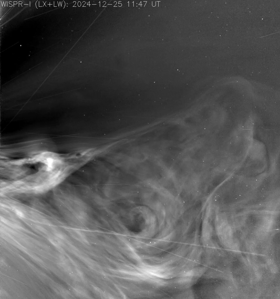
In addition to dominating the commercial and consumer market, CMOS imagers have been used as engineering cameras to enable the entry, descent, and landing of NASA’s Perseverance Mars rover, in the camera onboard the OCO-3 (Orbiting Carbon Observatory-3) mission that monitors the distribution of carbon dioxide on Earth, and as scientific imagers on NASA’s Parker Solar Probe mission that is revolutionizing our understanding of the Sun. CMOS imagers are on their way to Jupiter’s moon, Europa, on the agency’s Europa Clipper mission, and a delta-doped ultraviolet version with tailored response is under development for use on the upcoming UVEX (UltraViolet EXplorer) mission that will provide insight into how galaxies and stars evolve.
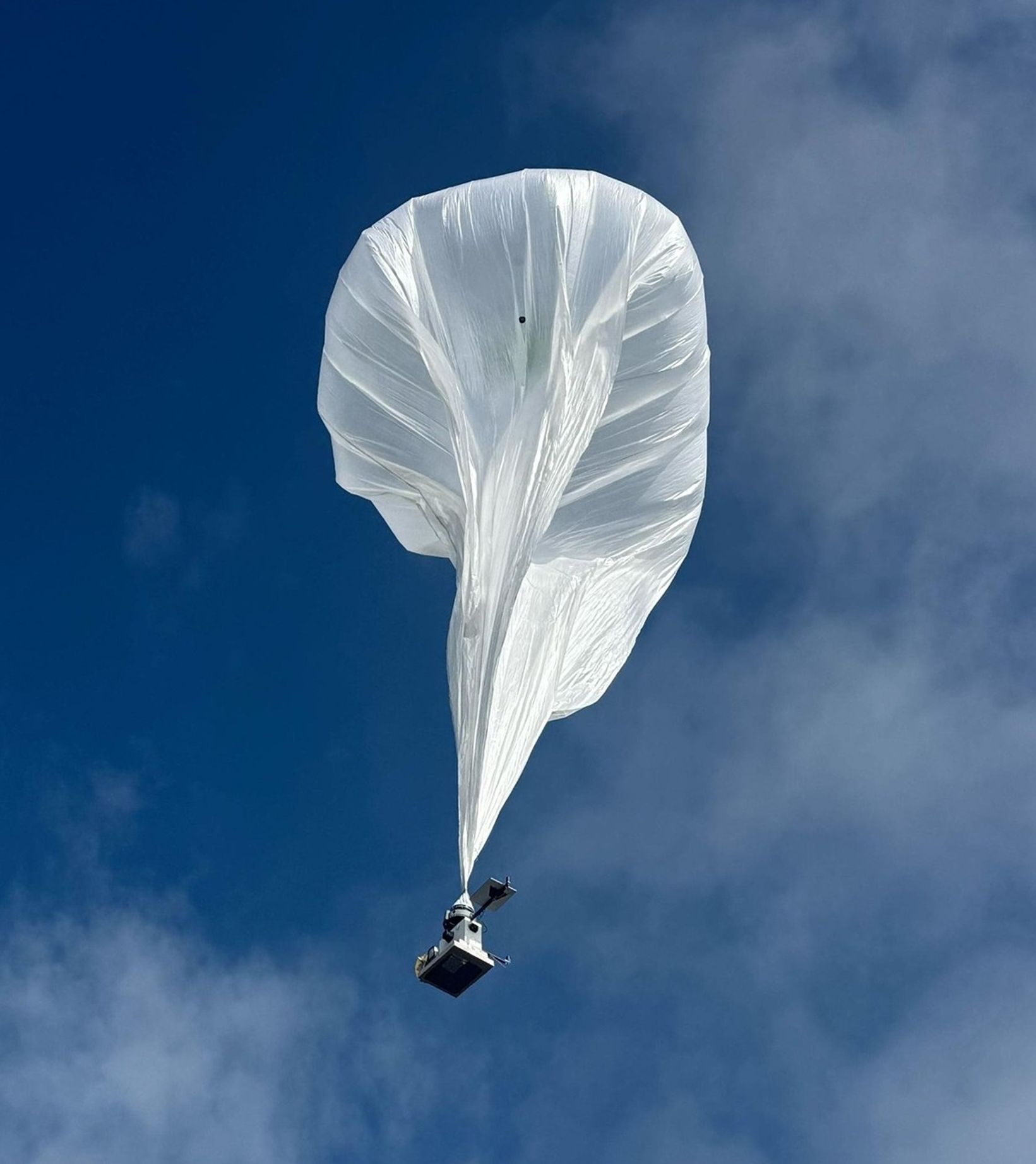
CMOS imagers are routinely used in monitoring the launch and deployment of CubeSats and SmallSats. They were recently used to monitor the deployment of Pandora, a small satellite that will characterize exoplanet atmospheres and their host stars; BLACKCAT (the Black Hole Coded Aperture Telescope), a small X-ray telescope; and the SPARCS (Star-Planet Activity Research CubeSat) mission designed to monitor and characterize the stellar flares of low-mass stars in ultraviolet to provide context for the habitability of exoplanets in their system. NASA is also developing descendants of this technology for use in missions that will search for life beyond Earth like its Habitable Worlds Observatory.
In recognition of the impact this CMOS technology has had, the National Academy of Engineering (NAE) has named Dr. Fossum the recipient of the 2026 Charles Stark Draper Prize for Engineering “for innovation, development, and commercialization of the complementary metal-oxide semiconductor (CMOS) active pixel image sensor ‘camera-on-a-chip.’” The NAE bestows this award biennially to honor an engineer “whose accomplishment has significantly impacted society by improving the quality of life, providing the ability to live freely and comfortably, and/or permitting the access to information.”
Sponsoring Organizations: The original efforts at JPL to develop this CMOS technology were funded by JPL and NASA.
Share
Details
Related Terms
Explore More


Related Posts


Stay Informed With the Latest & Most Important News
Previous Post
Next Post


Advertisement
-
 01Two Black Holes Observed Circling Each Other for the First Time
 -
 02From Polymerization-Enabled Folding and Assembly to Chemical Evolution: Key Processes for Emergence of Functional Polymers in the Origin of Life
 -
 03Astronomy 101: From the Sun and Moon to Wormholes and Warp Drive, Key Theories, Discoveries, and Facts about the Universe (The Adams 101 Series)
 -
 04True Anomaly hires former York Space executive as chief operating officer
 -
 05Φsat-2 begins science phase for AI Earth images
 -
 06Hurricane forecasters are losing 3 key satellites ahead of peak storm season − a meteorologist explains why it matters
 -
 07Binary star systems are complex astronomical objects − a new AI approach could pin down their properties quickly